- 您现在的位置:买卖IC网 > Sheet目录2008 > MAX1166BEUP+ (Maxim Integrated Products)IC ADC 16BIT 165KSPS 20-TSSOP
MAX1165/MAX1166
Low-Power, 16-Bit Analog-to-Digital Converter
with Parallel Interface
_______________________________________________________________________________________
7
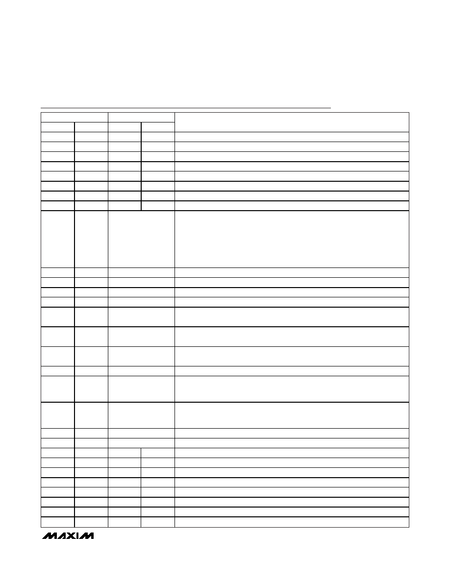
Pin Description
PIN
NAME
MAX1165
MAX1166
MAX1165
MAX1166
FUNCTION
1
D8
D4/D12
Three-State Digital Data Output
2
D9
D5/D13
Three-State Digital Data Output
3
D10
D6/D14
Three-State Digital Data Output
4
D11
D7/D15
Three-State Digital Data Output. D15 is the MSB.
5
—
D12
—
Three-State Digital Data Output
6
—
D13
—
Three-State Digital Data Output
7
—
D14
—
Three-State Digital Data Output
8
—
D15
—
Three-State Digital Data Output (MSB)
95
R/C
Read/Convert Input. Power up and put the MAX1165/MAX1166 in acquisition mode
by holding R/C low during the first falling edge of CS. During the second falling
edge of CS, the level on R/C determines whether the reference and reference
buffer power down or remain on after conversion. Set R/C high during the second
falling edge of CS to power down the reference and buffer, or set R/C low to leave
the reference and buffer powered up. Set R/C high during the third falling edge of
CS to put valid data on the bus.
10
6
EOC
End of Conversion. EOC drives low when conversion is complete.
11
7
AVDD
Analog Supply Input. Bypass with a 0.1F capacitor to AGND.
12
8
AGND
Analog Ground. Primary analog ground (star ground).
13
9
AIN
Analog Input
14
10
AGND
Analog Ground. Connect pin 14 to pin 12 (MAX1165). Connect pin 10 to pin 8
(MAX1166).
15
11
REFADJ
Reference Buffer Output. Bypass REFADJ with a 0.1F capacitor to AGND for internal
reference mode. Connect REFADJ to AVDD to select external reference mode.
16
12
REF
Reference Input/Output. Bypass REF with a 4.7F capacitor to AGND for internal
reference mode. External reference input when in external reference mode.
17
—
RESET
Reset Input. Logic high resets the device.
—
13
HBEN
High-Byte Enable Input. Used to multiplex the 14-bit conversion result:
1: Most significant byte available on the data bus.
0: Least significant byte available on the data bus.
18
14
CS
Convert Start. The first falling edge of CS powers up the device and enables
acquire mode when R/C is low. The second falling edge of CS starts conversion.
The third falling edge of CS loads the result onto the bus when R/C is high.
19
15
DGND
Digital Ground
20
16
DVDD
Digital Supply Voltage. Bypass with a 0.1F capacitor to DGND.
21
17
D0
D0/D8
Three-State Digital Data Output
22
18
D1
D1/D9
Three-State Digital Data Output
23
19
D2
D2/D10
Three-State Digital Data Output
24
20
D3
D3/D11
Three-State Digital Data Output
25
—
D4
—
Three-State Digital Data Output
26
—
D5
—
Three-State Digital Data Output
27
—
D6
—
Three-State Digital Data Output
28
—
D7
—
Three-State Digital Data Output
发布紧急采购,3分钟左右您将得到回复。
相关PDF资料
MAX1168BCEG+
IC ADC 16BIT 200KSPS 24-QSOP
MAX1183ECM+TD
IC ADC 10BIT 40MSPS DL 48-TQFP
MAX1184ECM+TD
IC ADC 10BIT 20MSPS DL 48-TQFP
MAX1186ECM+TD
IC ADC 10BIT 40MSPS DL 48-TQFP
MAX1187CCUI+
IC ADC 16BIT 135KSPS 28-TSSOP
MAX118EAI+
IC ADC 8BIT 1MSPS 28-SSOP
MAX1191ETI+T
IC ADC 8BIT 7.5MSPS DL 28-TQFN
MAX1192ETI+T
IC ADC 8BIT 22MSPS DL 28-TQFN
相关代理商/技术参数
MAX1166BEUP+T
功能描述:模数转换器 - ADC 16-Bit 165ksps 5.25V Precision ADC RoHS:否 制造商:Texas Instruments 通道数量:2 结构:Sigma-Delta 转换速率:125 SPs to 8 KSPs 分辨率:24 bit 输入类型:Differential 信噪比:107 dB 接口类型:SPI 工作电源电压:1.7 V to 3.6 V, 2.7 V to 5.25 V 最大工作温度:+ 85 C 安装风格:SMD/SMT 封装 / 箱体:VQFN-32
MAX1166BEUP-T
功能描述:模数转换器 - ADC RoHS:否 制造商:Texas Instruments 通道数量:2 结构:Sigma-Delta 转换速率:125 SPs to 8 KSPs 分辨率:24 bit 输入类型:Differential 信噪比:107 dB 接口类型:SPI 工作电源电压:1.7 V to 3.6 V, 2.7 V to 5.25 V 最大工作温度:+ 85 C 安装风格:SMD/SMT 封装 / 箱体:VQFN-32
MAX1166CCUP
功能描述:模数转换器 - ADC RoHS:否 制造商:Texas Instruments 通道数量:2 结构:Sigma-Delta 转换速率:125 SPs to 8 KSPs 分辨率:24 bit 输入类型:Differential 信噪比:107 dB 接口类型:SPI 工作电源电压:1.7 V to 3.6 V, 2.7 V to 5.25 V 最大工作温度:+ 85 C 安装风格:SMD/SMT 封装 / 箱体:VQFN-32
MAX1166CCUP-T
功能描述:模数转换器 - ADC RoHS:否 制造商:Texas Instruments 通道数量:2 结构:Sigma-Delta 转换速率:125 SPs to 8 KSPs 分辨率:24 bit 输入类型:Differential 信噪比:107 dB 接口类型:SPI 工作电源电压:1.7 V to 3.6 V, 2.7 V to 5.25 V 最大工作温度:+ 85 C 安装风格:SMD/SMT 封装 / 箱体:VQFN-32
MAX1166CEUP
功能描述:模数转换器 - ADC RoHS:否 制造商:Texas Instruments 通道数量:2 结构:Sigma-Delta 转换速率:125 SPs to 8 KSPs 分辨率:24 bit 输入类型:Differential 信噪比:107 dB 接口类型:SPI 工作电源电压:1.7 V to 3.6 V, 2.7 V to 5.25 V 最大工作温度:+ 85 C 安装风格:SMD/SMT 封装 / 箱体:VQFN-32
MAX1166CEUP-T
功能描述:模数转换器 - ADC RoHS:否 制造商:Texas Instruments 通道数量:2 结构:Sigma-Delta 转换速率:125 SPs to 8 KSPs 分辨率:24 bit 输入类型:Differential 信噪比:107 dB 接口类型:SPI 工作电源电压:1.7 V to 3.6 V, 2.7 V to 5.25 V 最大工作温度:+ 85 C 安装风格:SMD/SMT 封装 / 箱体:VQFN-32
MAX1167
制造商:MAXIM 制造商全称:Maxim Integrated Products 功能描述:Multichannel, 16-Bit, 200ksps Analog-to-Digital Converters
MAX1167_09
制造商:MAXIM 制造商全称:Maxim Integrated Products 功能描述:Multichannel, 16-Bit, 200ksps Analog-to-Digital Converters